
 العربية
 Español
 中文
中文 Deutsch
 Français
 Português
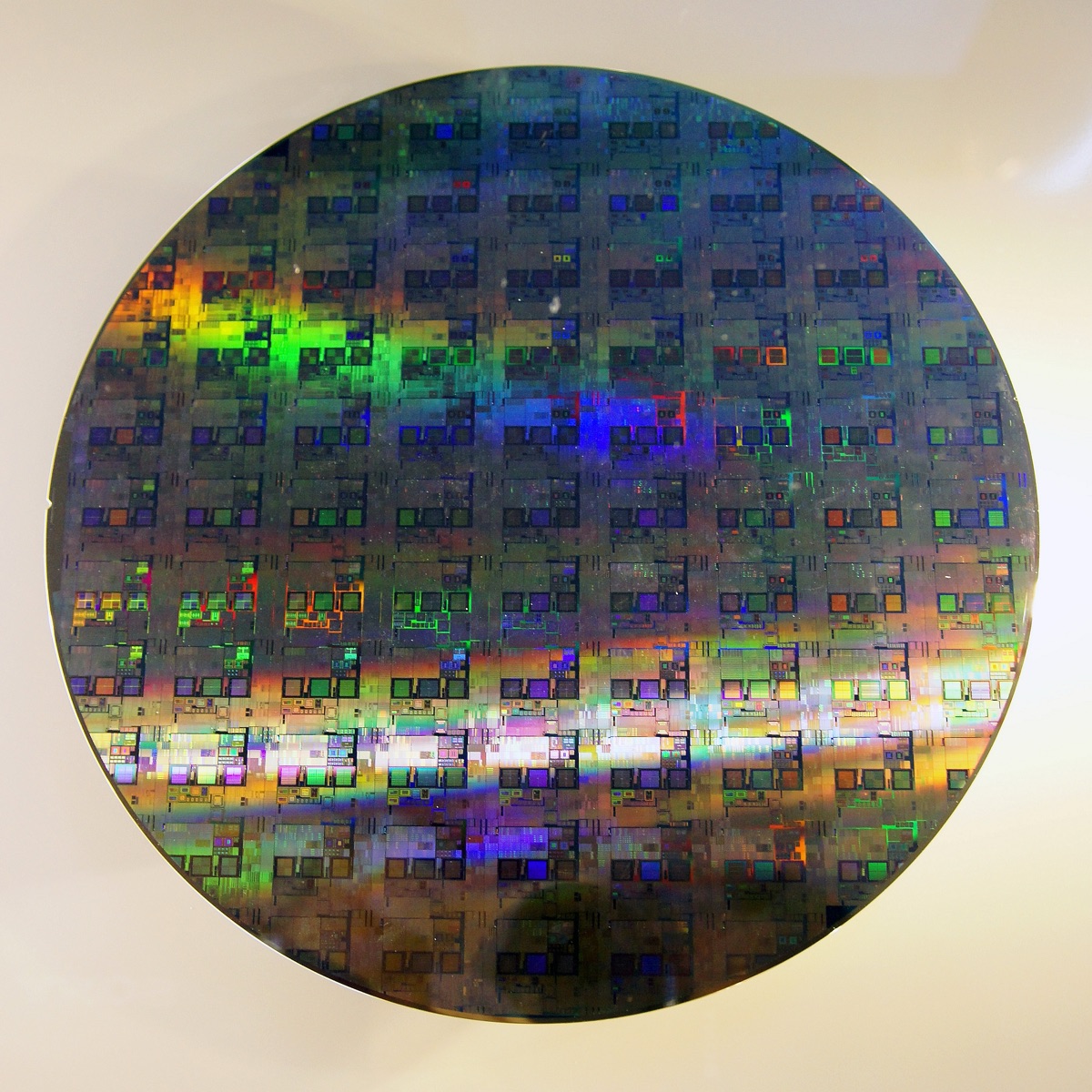
For sixty years, the story of computing has been the same quiet miracle: every couple of years, engineers find a way to fit roughly twice as many transistors into the same sliver of silicon. That doubling - Moore’s Law - is the reason a phone in your pocket outguns the supercomputers of the 1990s. It has also been declared dead more times than almost any idea in technology. On June 25, 2026, IBM offered the latest reason to bet on its survival: at the VLSI Symposium, the company unveiled what it calls the world’s first sub-1-nanometer chip technology - a 0.7nm (7-angstrom) node built on a new three-dimensional architecture it calls NanoStack. It is a research milestone, not a product you can buy. But it is a credible map for another decade of progress.
- What: the world’s first sub-1nm chip technology - a 0.7nm (7-angstrom) node
- Who / when / where: IBM, on June 25, 2026, at the VLSI Symposium; developed at IBM’s Albany NanoTech complex, New York
- The architecture: NanoStack - the industry’s first 3D, nanosheet-based design, vertically stacking complementary transistors (CFET)
- Density: nearly 100 billion transistors on a fingernail-sized chip - about 2x IBM’s 2021 2nm chip
- Gains: up to 50% more performance OR up to 70% greater energy efficiency vs the 2nm node; 40% denser SRAM
- The runway: IBM says the design supports at least another decade of scaling
- The catch: “0.7nm” is a naming convention, not a physical size; production is roughly 5 years away
1. What IBM Announced
IBM’s researchers say they have demonstrated working logic at a 0.7-nanometer, or 7-angstrom, node - the first time the industry has crossed below the one-nanometer threshold in a named process technology. The headline figure: nearly 100 billion transistors packed onto a chip about the size of a fingernail, roughly double the density of the 2nm chip IBM introduced in 2021.
Compared with that 2nm generation, IBM reports the new node can be tuned for either up to 50% higher performance at the same power, or up to 70% better energy efficiency at the same speed - a trade-off chip designers dial in for a given application. It also delivers 40% scaling in SRAM, the fast on-chip memory that has been notoriously hard to shrink and that increasingly bottlenecks AI accelerators.
“With our new nanostack architecture, we’re not just making smaller transistors. We’re reinventing how chips are built,” said Jay Gambetta, Director of IBM Research, who described the result as “a landmark moment in computing, pushing technology beyond the nanometer era to the scale of atoms.”
2. Wait - What Does “0.7 Nanometer” Actually Mean?
Here is the part worth being honest about, because it is widely misunderstood. A nanometer is one-billionth of a meter; an angstrom is one-tenth of a nanometer - roughly the width of a single atom. So a literal 0.7-nanometer transistor would be about seven atoms across, which is not what is being built. Modern node names like “5nm,” “3nm,” “2nm” and now “0.7nm” are marketing labels that no longer correspond to any single physical dimension on the chip. They are a shorthand for a generation of density and performance, not a ruler measurement.
Until about 2011, a node’s number really did track a key feature size. Then transistors went 3D and the geometry got too complicated for one number to capture, so the labels became generational names instead. What matters is the real outcome: more transistors, more speed, and less energy per operation. By that measure, IBM’s “0.7nm” is a genuine step beyond “2nm” - the marketing label simply rounds a complex achievement into a single tidy figure.
3. The NanoStack Idea: Building Up Instead of Out
For decades, the way to fit more transistors was to make each one smaller and place them side by side. That horizontal shrinking is running into atomic limits. IBM’s answer is to build upward. NanoStack uses a structure called a complementary field-effect transistor (CFET): it takes the two transistor types every logic chip needs - one that switches on with positive charge (PFET) and one with negative (NFET) - and stacks them on top of each other instead of laying them next to each other. Doing so frees up the horizontal space they used to occupy, which is where much of the density gain comes from.
The channels themselves are vanishingly thin: IBM’s design uses stacks of nanosheets each only about 15 atoms thick, spaced roughly 9 nanometers apart, with the gate material wrapping completely around each sheet for precise control of the electrical current. It is the latest move in a long evolution of how a transistor is shaped.
| Architecture | Era | The big idea |
|---|---|---|
| Planar | until ~2011 | A flat transistor with the gate sitting on top |
| FinFET | ~2011 on | A vertical fin-shaped channel; the gate wraps three sides |
| Gate-All-Around (nanosheet) | IBM 2nm, 2021 | The gate wraps the channel on all four sides for tighter control |
| NanoStack (CFET) | IBM, 2026 | Stack the two transistor types vertically to reclaim horizontal space |
4. The Leap Since 2021
IBM has form here. In May 2021 it announced the world’s first 2nm chip, fitting 50 billion transistors on a fingernail using Gate-All-Around nanosheets - the architecture that has since become the industry’s leading edge. NanoStack roughly doubles that density and reframes the recipe.
| Metric | IBM 2nm (2021) | IBM 0.7nm NanoStack (2026) |
|---|---|---|
| Transistors (fingernail-sized chip) | ~50 billion | ~100 billion |
| Architecture | Gate-All-Around nanosheet | 3D NanoStack (stacked CFET) |
| Performance vs 2nm | baseline | up to +50% |
| Energy efficiency vs 2nm | baseline | up to +70% |
| SRAM scaling | - | +40% |
That 50%/70% split is the same kind of dial IBM offered with 2nm (which it pitched as up to 45% more performance or 75% less energy than 7nm). Designers rarely take all of one or the other; they balance speed and power for the job at hand - a phone leans toward efficiency, a data-center AI chip toward throughput.
5. Why It Matters: AI, Energy, and the Survival of Moore’s Law
The timing is everything. Artificial intelligence has turned compute into one of the world’s scarcest resources, and the limiting factor is increasingly energy: data centers are straining power grids, and every percent of efficiency compounds across millions of chips. A node that offers up to 70% better energy efficiency - and 40% denser SRAM, exactly the memory AI models hammer - lands squarely on the industry’s biggest bottleneck.
It also answers, for now, the recurring fear that Moore’s Law has finally hit the wall. By moving from shrinking transistors to stacking them, IBM opens a new axis of scaling that does not depend on making features ever-smaller. As one semiconductor-industry analyst put it, the approach “puts another 10 to 15 years on the roadmap.” IBM’s own roadmap projects at least a decade of further scaling built on NanoStack.
In 1965, Intel co-founder Gordon Moore observed that the number of transistors on a chip was doubling about every two years, and predicted it would continue. It is not a law of physics but a self-fulfilling industry rhythm - and it is the engine behind decades of exponential improvement in computing. Each new generation has been harder to deliver than the last, which is why a credible new path like NanoStack is treated as such a big deal.
6. The Road to the Factory
This is a laboratory breakthrough, and IBM is clear-eyed about the distance to mass production. The company’s earliest realistic path to commercial chips is roughly five years out, and getting there means solving real manufacturing problems - chiefly the yield challenges of reliably stacking transistor layers, and tight thermal-budget limits (many steps must stay below about 400°C so earlier layers are not damaged). To bridge that gap, IBM is working with an ecosystem of equipment and materials partners, including ASML (the maker of the High-NA EUV lithography tools that print the finest features), Lam Research, Tokyo Electron and SCREEN.
IBM is not alone in chasing the CFET concept - Intel, Samsung, TSMC and the European research hub imec are all exploring stacked complementary transistors as the next step after Gate-All-Around. IBM’s claim to being first rests on its specific NanoStack implementation and the staggered way it aligns the stacked layers. Gambetta framed the ambition simply: “I hope to see it be as successful as the 2-nanometer [chip] and become the industry platform.”
What We Still Don’t Know
- Whether it manufactures at scale. Lab demonstrations and high-yield, high-volume production are very different things; stacking adds steps and complexity.
- How close the real-world gains land to the headline “up to 50%/70%” once full chips, interconnects and packaging are built around the transistors.
- The exact timeline. “About five years” to production is a target, and leading-edge schedules routinely move.
- Who ships first. With Intel, Samsung, TSMC and imec all pursuing CFET, the order in which stacked transistors reach real products is still open.
None of that dims the headline. After years of warnings that the shrinking was over, IBM has shown a concrete way to keep computing’s defining trend going - by building up where building smaller ran out of room.
Sources
- IBM Newsroom: IBM Debuts World’s First Sub-1 Nanometer Chip Technology (June 25, 2026)
- MIT Technology Review: IBM unveils chip technology that could extend Moore’s Law another decade
- Live Science: IBM creates first sub-1nm computer chip - 100 billion transistors
- IBM Newsroom (2021): IBM Unveils World’s First 2 Nanometer Chip Technology · HPCwire: 2nm test chip with 50 billion transistors
Curated by Jerry Cards - jerrycards.com. We research the week’s most consequential tech, science, and business news so you don’t have to. More at jerrycards.com/news. Representative image: a 300mm silicon wafer by Wikimedia Commons user Peellden, licensed CC BY-SA 3.0.