
 العربية
 Español
 中文
中文 Deutsch
 Français
 Português
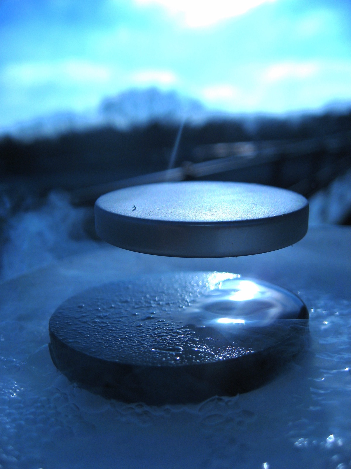
Sometimes the cleverest way to improve a material is not to change the material at all - but to change the floor it grows on. An international team led by physicists at Chalmers University of Technology has shown that carving nanoscale ridges into the surface beneath an ultrathin superconductor makes it markedly tougher: it stays superconducting at a higher temperature and shrugs off far stronger magnetic fields. Most striking of all, a film just 10 nanometres thick - five times thinner than the usual reference - ended up outperforming the thicker one. The trick is pure geometry, and it hands physicists an entirely new design knob for one of the most useful phenomena in nature.
Here is what the team did, what improved and by how much, why it works, and why it could matter for everything from quantum computers to MRI scanners.
- Who: an international team led by Chalmers University of Technology (Sweden), with partners in Italy, India, France and Germany
- What: grew ultrathin films of the cuprate superconductor YBCO on a magnesium-oxide surface sculpted into nanoscale ridges
- Onset temperature: more than 15 K higher (rising to around 90 K) than in standard thicker films
- Magnetic-field tolerance: upper critical field more than 50 tesla higher
- The proof: an identical film on a flat substrate showed no improvement - the gain is geometric
- Published: Nature Communications, 7 January 2026 (DOI 10.1038/s41467-025-67500-2)
1. The Idea: Sculpt the Surface, Not the Chemistry
In the copper-oxide (cuprate) superconductors, the number of charge carriers - the doping level - is locked in when the crystal is made. Unlike a modern 2D-material transistor, you cannot simply dial it up and down with a gate voltage. So physicists have been hunting for other levers, and one of the most promising is strain: gently stretching or squeezing the crystal lattice to nudge the delicate competition between superconductivity and other electronic orders.
The Chalmers-led team found a particularly elegant way to apply that lever. They started with a substrate of magnesium oxide (MgO) cut along its (110) face and heated it to about 790 °C. At that temperature the surface spontaneously reorganises - it reconstructs - into a quasi-regular washboard of nanoscale ridges and valleys, with ridges roughly 1 nanometre tall and 20-50 nanometres wide. Then they deposited a film of YBCO (YBa2Cu3O7−δ) only 10 nanometres thick on top, so the superconductor settled over the carved landscape like snow over a corrugated roof.
2. The Numbers
Compared with a conventional 50-nanometre film at the same fixed (under)doping of p ≈ 0.125, the thin film on the nanofaceted surface did not just match it - it beat it on the two measures that matter most for real devices.
| Property | Standard film (50 nm) | 10 nm film on nanofaceted MgO |
|---|---|---|
| Film thickness | 50 nm | 10 nm (5x thinner) |
| Superconducting onset temperature | ~75 K | ~90 K (more than 15 K higher) |
| Upper critical magnetic field | baseline | more than 50 T higher (largest gains near p ≈ 0.145) |
| Charge-density-wave order | two directions (bidirectional) | one direction (unidirectional) |
- YBCO: yttrium barium copper oxide, a famous high-temperature superconductor and the first that could be cooled with cheap liquid nitrogen (which boils at 77 K, or −196 °C).
- Onset temperature: the temperature at which a material begins to lose all electrical resistance and turn superconducting. Higher is better - it means less extreme cooling.
- Upper critical field: the magnetic field strong enough to destroy superconductivity. Higher is better - the superconductor keeps working inside powerful magnets.
- Tesla: a unit of magnetic-field strength. A hospital MRI runs at 1.5-3 T, so a 50-tesla improvement is enormous.
3. The Surprise: Thinner Should Be Worse
This is the part that makes physicists sit up. As a rule, making a superconducting film thinner degrades it - the superconductivity weakens and its transition temperature falls. Yet here the ultrathin 10-nanometre film not only recovered that lost ground, it overtook a film five times thicker. The conclusion is that the nanofaceted surface is doing something genuinely new to the electrons, not merely avoiding the usual thin-film penalty.
4. Why It Works: Reshaping the Electrons
In cuprates, superconductivity shares the stage with a rival called a charge-density wave (CDW) - a static ripple in the electron density that competes with the superconducting state for the same electrons. In an ordinary film, that ripple runs in two directions at once. The team found that the carved substrate breaks the tie.
- The film couples most strongly to the substrate right at the sharp ridge tips, where under-coordinated MgO atoms sit. This imprints a directional strain on the copper-oxide planes above.
- That strain makes the electrons nematic - they start to favour one crystal axis over the other (the measured effective masses become strongly anisotropic instead of equal).
- The charge-density wave, which normally runs both ways, is suppressed along one axis and left intact along the other, turning it unidirectional.
- With its main competitor cut down in one direction, superconductivity strengthens - surviving to higher temperatures and far higher magnetic fields.
5. The Control That Clinches It
How do you know the ridges are responsible, and not some subtler thickness effect? The team ran the obvious test. They grew the same 10-nanometre and 50-nanometre YBCO films on strontium titanate (SrTiO3), a substrate whose surface does not reconstruct into facets at high temperature. On that flat surface, the thin and thick films had the same onset temperature - no enhancement at all. The boost appears only when the sculpted nanofacets are present, which is about as clean a piece of cause-and-effect as condensed-matter physics offers.
6. Why It Matters
Superconductors are the closest thing we have to a free lunch in electricity: they carry current with zero resistance, so no energy is wasted as heat. That is why they sit at the heart of MRI scanners, maglev trains, particle accelerators, experimental fusion reactors, and the wiring of some quantum computers. Two stubborn limits hold them back - they must be kept very cold, and a strong enough magnetic field switches them off.
This result takes direct aim at the second limit. Pushing the upper critical field up by more than 50 tesla means a superconductor that keeps working deep inside the powerful magnets where it is most useful. And because the lever is geometry - the shape of the surface underneath, something chip-makers already know how to pattern - it slots naturally into existing fabrication thinking. The authors frame it as a new paradigm: substrate engineering as a tool to tune and strengthen superconductivity, potentially beyond cuprates to other strongly correlated materials.
7. The Honest Caveats
- Still cold. This is not a room-temperature superconductor. YBCO here still operates around 90 K (liquid-nitrogen territory); the achievement is making thin-film superconductivity tougher, not warm.
- Lab-scale films. The work is on carefully grown research films, not yet on the kilometres of wire or the device geometries that real magnets and chips demand.
- From mechanism to product takes time. Turning a clean physical principle into manufacturable technology is a long road - but a clear, controllable mechanism is exactly the foundation that road needs.
What We Still Do Not Know
- How far the idea generalises - whether nanofaceted substrates can boost other superconductors and other quantum materials, as the authors hope.
- Whether the effect survives in thicker, device-relevant films, or is special to the ultrathin limit.
- How precisely the ridge size, spacing and orientation can be tuned to dial in a target performance.
Sources
- E. Wahlberg, R. Arpaia, F. Lombardi et al., Boosting superconductivity in ultrathin YBa2Cu3O7−δ films via nanofaceted substrates, Nature Communications (7 Jan 2026), DOI 10.1038/s41467-025-67500-2 · open-access full text (PMC)
- Chalmers University of Technology: Superconductor advance could unlock ultra-energy-efficient electronics · EurekAlert release · ScienceDaily coverage
- Image: magnet levitating above a cooled YBa2Cu3O7 superconductor (Meissner effect), by Julien Bobroff and Frederic Bouquet, LPS / Universite Paris-Saclay, via Wikimedia Commons, licensed CC BY-SA 3.0.
Curated by Jerry Cards - jerrycards.com. We read the week most consequential science, tech and business research so you do not have to. More at jerrycards.com/news.